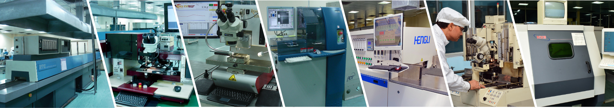
VLSI and MEMS Packaging facility operating in Class 100 and Class 10000 Clean Rooms includes Die Bonders, Ball and Wedge Wire Bonders, Multi-Zone Furnaces for Hermetic Sealing, Multi-Function Bond Pull Testers, Laser Welder, Dicing Saw, Tape Mounter etc.
Key capabilities
-
Package design lab catering the bonding and device drawing generations for all devices for post Fab activities.
-
Design and analysis of Single die and multi-die substrates (SiP) to optimise the Signal and Power Integrity performances for CMOS, Imager & RF devices.
-
Design, analysis and development for MEMS packaging
-
Thermo-mechanical design, analysis & characterisation for devices
-
Layout of IC package and generation of fabrication inputs for developing custom package.
-
Standard IC packages and Custom Substrate development end to end solutions.
-
Fine Pitch Bonding capability (using 0.8,1 &1.25mil wire) for pad size of 57µmx57µm and 65µm pitch
-
Low Temperature Process for packaging large dies of Imager devices
-
Multi-Chip Packaging Process for ASICs and sensor devices
Software
-
Cadence APD
-
Cadence Sigrity
-
Ansys Mechanical
-
AutoCad
-
SolidWorks